7月8日のお知らせ「キャンセル待ち含めて、お申込み受付を終了いたしました。多数のお申込みどうもありがとうございました。」
More ...
化学物理工学科 Applied Physics & Chemical Engineering
国立大学法人東京農工大学 TUAT Tokyo University of Agriculture & Technology
7月8日のお知らせ「キャンセル待ち含めて、お申込み受付を終了いたしました。多数のお申込みどうもありがとうございました。」
More ...
研究室の教育研究方針は、地球規模の社会問題(資源、水、食料生産、気候、生態系)に対して、学問として工学は何をすべきかを考えることである。to consider what engineering should do as an academic discipline to address global-scale social issues (resources, water, food production, climate, and ecosystems).
More ...
#1. Transport of heated liquid mixtures with colloidal fluorescent particles through multiple biomass layers/ 加熱された複数バイオマス層を通るコロイド状蛍光粒子と液体の輸送
#2. A chemical coating of clay-based soil particles slows evaporation.
粘土系土壌粒子の化学コーティングは水の蒸発を遅らせる
化学産業のスマート化と超スマート社会の実現に向けて、化学工学の知識と人工知能や最適化、シミュレーションの手法を駆使して、化学プラントの運転・制御を中心に、高品質な製品を高効率かつ安全に生産するための方法について研究しています。
More ...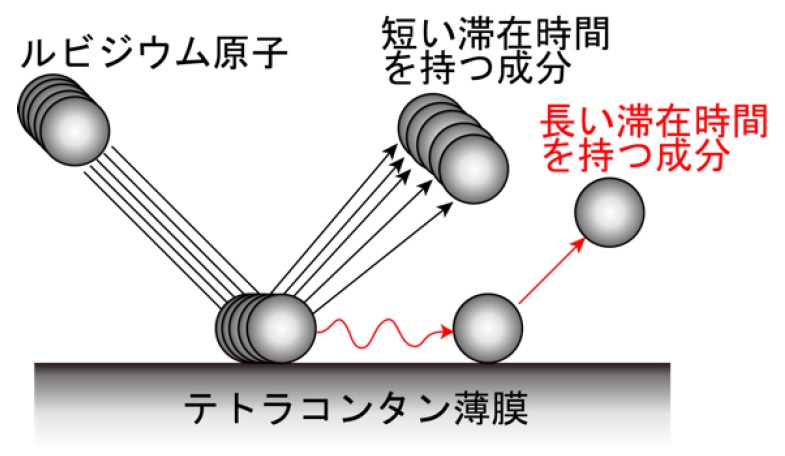
原子磁力計などに用いられるアルカリ金属原子の中に、スピン緩和防止コーティングに使われるパラフィンの表面での滞在時間が極端に長いものがあることを明らかにしました。Some alkali metal atoms have extremely long residence time on the surface coated with antispin relaxation coating.
More ...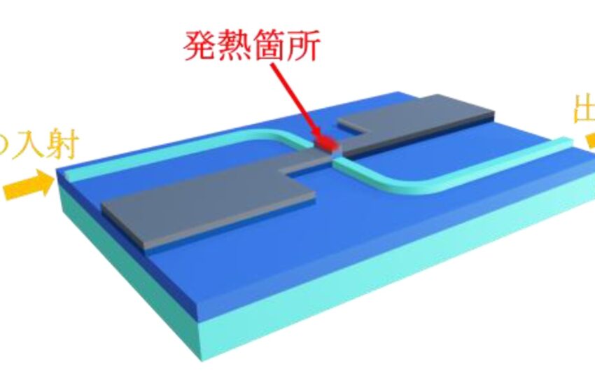
遷移金属のコバルトを積層したシリコン光導波路(Siプラズモニック導波路)の幅0.4マイクロメートルの領域に光が到達し、吸収された光によって243℃に加熱できることを金属の抵抗の変化から測定することに成功しました(清水研究室)。Shimizu Lab succeeded in measuring from the change in resistance of a metal that light reaches a region of 0.4
More ...模擬授業 A “model” lecture from open-campus (June 2021) by Prof. Hiromasa Shimizu
More ...
電子材料や医療等に利用される技術として、(目的の)基板表面に対して気中から微粒子を沈着させる技術がある。One of the technologies used in electronic materials and medicine is the deposition of fine particles from the air onto the (target) substrate surface.
More ...
Keywords: Soft-sensor, Virtual Sensing, Process Data Analysis, Statistical Process Control ソフトセンサ、バーチャルセンシング、プロセスデータ解析、統計的プロセス制御
More ...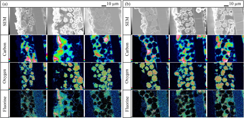
「液体浸透時間」法は、微粒子膜(例えば、リチウムイオン電池の電極)の内部構造を評価するための簡便で有用な方法です。”Liquid penetration time” method is a simple and useful method to evaluate the inner structures of particulate films (for example, Li-ion battery electrodes)
More ...
将来的に分析物の屈折率と吸収係数の両方を検知できる光センサが高感度化されることで、手のひらサイズの光集積回路やIoTセンサの実現が期待される。As optical sensors become more sensitive in the future, handy optical integrated circuits and IoT sensors are expected to be realized.
More ...