共振器と一体化したSiプラズモン導波路における288K局所光熱加熱と小型化の定量化 Quantification of 288 K local photothermal heating and miniaturization in Si plasmonic waveguides integrated with resonators (by Nana Ota, Kota Shinohara, Masahiko Hasumi and Hiromasa Shimizu) Japanese Journal of Applied Physics (2023) doi.org/10.35848/1347-4065/acc917
シリコンで光加熱!?:革新的なプラズモンデバイスへの新しいアプローチ
シリコンは光技術(フォトニクス)の分野で広く使用されている材料ですが、熱への変換効率が低く、光スイッチやデータ記憶、バイオセンサーのような熱を必要とするアプリケーションへの活用が制限されていました。では、この課題を克服し、光でシリコンを効率的に加熱できるデバイスを作ることはできるのでしょうか?
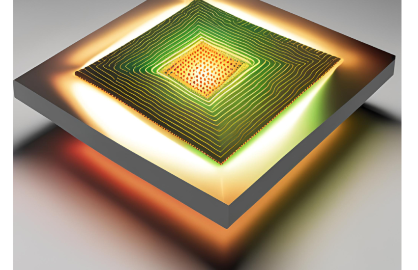
清水研究室は、この課題に対してシリコンプラズモン波導加熱器とリング共振器を組み合わせた新しい設計により解決しました。プラズモン波導は、金属層の電子集団振動と光を結びつけることで、ナノスケールで光を閉じ込め導く構造です。リング共振器は、導波路をループ状にしたもので、特定の波長で共鳴モードを作り出し、光強度を強化することができます。
研究者たちは金属層にコバルト (Co) を使用し、シリコン導波路とリング共振器に統合しました。光を導波路加熱器に入射すると、光の強度が高まるにつれて共鳴波長が長い波長側にシフトすることが観察されました。これは、コバルト層が光を吸収して温度が上昇したことを示します。研究者たちは、熱光効果に基づいてこのシフトを解析し、コバルト層の局所的な温度上昇を定量化しました。
入力光強度が 6.3 mW の場合、局所的な温度上昇は最大 288 K (15 °C) に達し、光熱変換効率は 46.1 K mW−1 でした。これらの値は従来のデバイスよりも高く、新しい加熱器が改善された性能を持っていることを示しています。研究者たちはさらに、局所的な温度上昇と光熱変換効率は、シリコン酸化物 (SiO2) バッファー層の厚さとリング共振器の半径に依存することを発見しました。これらの要因は、伝播する光とコバルト層との相互作用の強さと、リング共振器内部の光の等価強度に影響を与えることを説明しました。
研究者たちは、デバイス構造を再設計することで、より小型・低消費電力で高い効率を実現する方法について議論しました。SiO2 バッファー層を薄くし、リング半径を小さくし、コバルト層を短くすることで加熱性能を向上させることができると提案しています。また、光損失が低い金 (Au) や銀 (Ag) など他の金属の使用も検討しています。
開発されたプラズモン波導加熱器は、フォトニクス、ナノテクノロジー、バイオテクノロジーのさまざまな分野で応用できます。例えば、温度変化で光の透過を制御する小型光熱スイッチや、光を利用して材料を加熱磁化することでデータを記憶するオンチップ磁気光記録 (MO) や熱補助磁気記録 (HAMR) に使用できます。また、電流なしで加熱することにより、プラズモン光センサーへの吸着分子の脱着、DNAの熱泳動操作、ラボオンチップ方式でのポリメラーゼ連鎖反応による遺伝子複製なども可能になります。

How to heat up silicon with light: a new approach for plasmonic devices
Silicon is a widely used material for photonics, the science and technology of light. However, silicon has a limitation: it cannot efficiently convert light into heat, which is needed for some applications such as optical switches, data storage, and biosensors. How can we overcome this challenge and create devices that can heat up silicon with light?
Shimizu Research Group has found a solution: they designed and fabricated silicon plasmonic waveguide heaters with ring resonators. Plasmonic waveguides are structures that can confine and guide light at the nanoscale, by coupling it with the collective oscillations of electrons in a metal layer. Ring resonators are loops of waveguides that can enhance the light intensity and create resonant modes with specific wavelengths.
The researchers used cobalt (Co) as the metal layer, and integrated it with silicon waveguides and ring resonators. They injected transverse magnetic ™ mode light into the waveguide heaters, and observed that the resonance wavelength shifted toward a longer wavelength as the light intensity increased. This shift indicated that the temperature of the Co layer rose due to the absorption of light. By analyzing the shift based on the thermo-optic effect, the researchers quantified the local temperature rise at the Co layer.
They found that the local temperature rise was as high as 288 K (15 °C) when the input power was 6.3 mW, and the photothermal conversion efficiency was 46.1 K mW−1. These values were higher than those of previous devices, showing that the plasmonic waveguide heaters had improved characteristics. The researchers also found that the local temperature rise and the photothermal conversion efficiency depended on the thickness of the silicon dioxide (SiO2) buffer layer, and the radius of the ring resonator. They explained that these factors affected the strength of the interaction between the propagating light and the Co layer, and the equivalent light intensity inside the ring resonator.
The researchers discussed how to achieve a higher efficiency with a smaller size and a lower input power, by redesigning the device structure. They suggested that using a thinner SiO2 buffer layer, a smaller ring radius, and a shorter Co layer could enhance the heating performance. They also proposed to use other metals such as gold (Au) or silver (Ag), which have lower optical losses than Co.
The plasmonic waveguide heaters developed by the researchers could have various applications in the fields of photonics, nanotechnology, and biotechnology. For example, they could be used for compact photothermal switches, which can control the transmission of light by changing the temperature. They could also be used for on-chip magneto-optical (MO) recording or heat-assisted magnetic recording (HAMR), which can store data by using light to heat up and magnetize a material. Moreover, they could be used for heating without electric current, which could enable the desorption of adsorbed molecules in plasmonic optical sensors, the thermophoretic manipulation of DNA, and the gene replication by polymerase chain reaction with the lab-on-a-chip scheme.